In today’s world of wearables, medical devices, and IoT sensors, size isn’t just a design choice — it’s a competitive advantage. As products become smaller, smarter, and more powerful, manufacturers are increasingly turning to advanced packaging technologies such as Die-Sized (DS) BGAs and Wafer-Level Chip-Scale Packages (WLCSPs) to deliver breakthrough performance in the tiniest of footprints.
At ADAPT ems, we’ve seen this trend accelerate rapidly among our customers, all of whom are chasing the same goals: miniaturization, performance, and cost efficiency.
Why DS BGAs and WLCSPs?
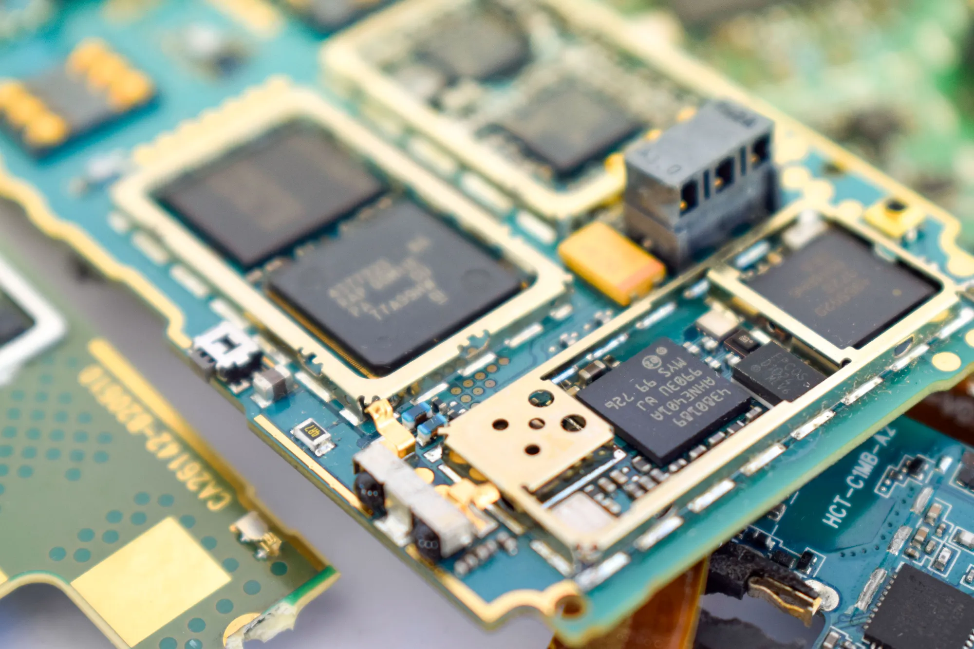
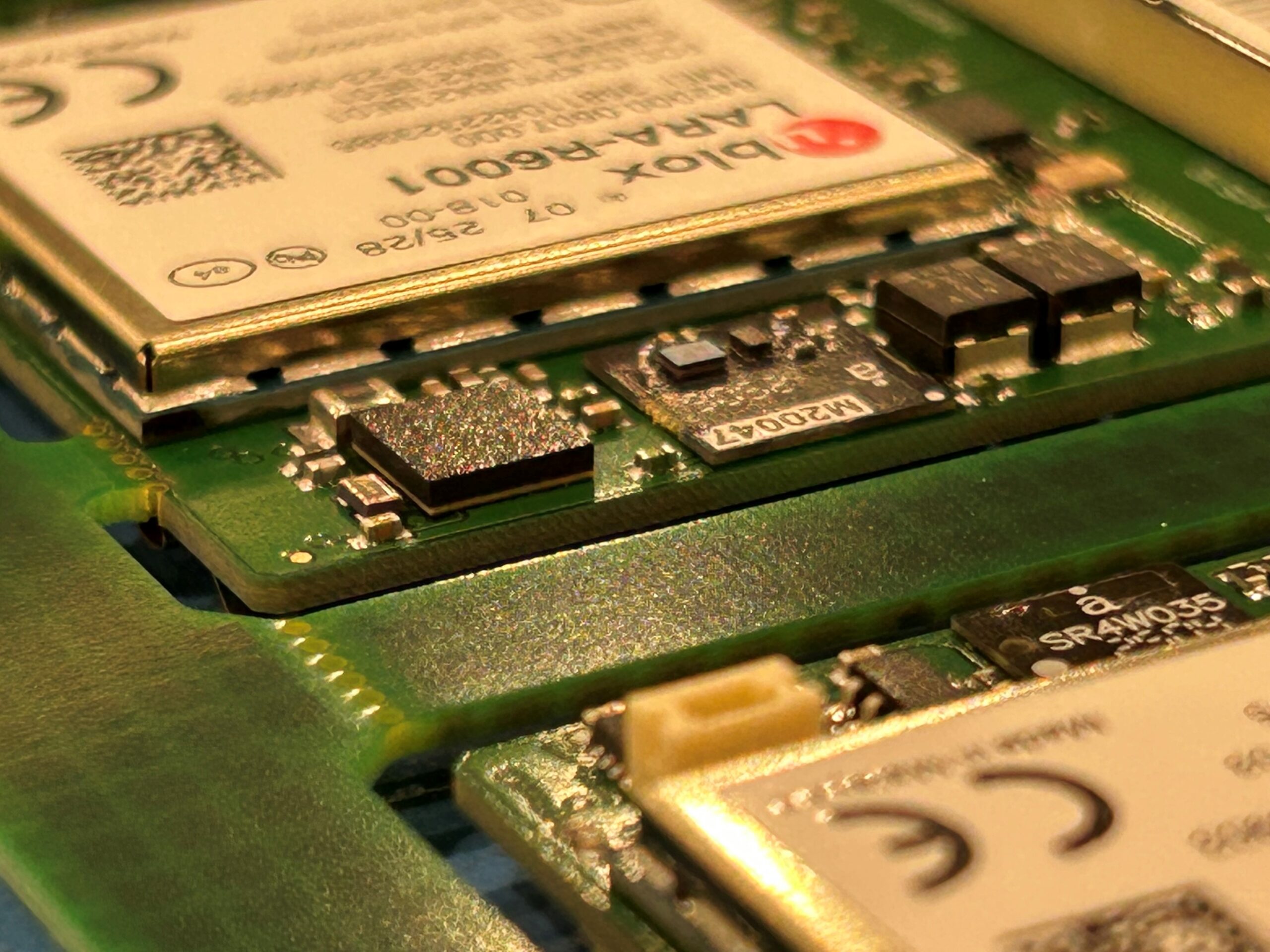
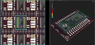
These cutting-edge devices are remarkable because the package is no larger than the silicon die itself. This means designers can pack dozens of I/Os into a mere 1–2 mm² area, using fine-pitch solder balls at <0.3 mm pitch.
The benefits are clear:
It’s no surprise they’re becoming the go-to solution for innovators pushing boundaries in electronics.
The Challenge of Going Smaller
But with great performance comes new challenges. Successfully designing and manufacturing with DS BGAs and WLCSPs requires:
Simply put: you need to get it right the first time. And that’s where ADAPT ems makes the difference.
Our Proven Approach
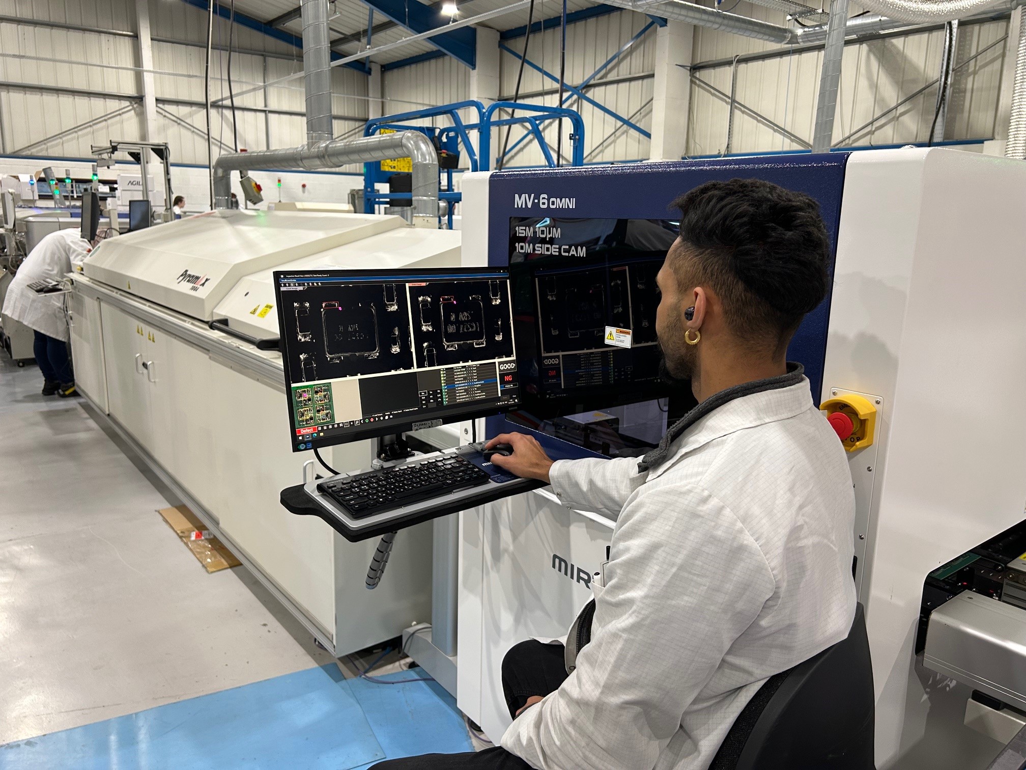
At ADAPT ems, precision and reliability are at the core of what we do. We’ve invested heavily in the people, processes, and technology that allow us to place these advanced devices at scale — and with industry-leading accuracy.
Here’s how we deliver:
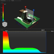
The results speak for themselves: we’ve placed tens of thousands of DS BGAs and WLCSPs with an extraordinary >99.93% Right-First-Time yield at the PCBA level.
Why Partner with ADAPT ems?
When it comes to cutting-edge miniaturization, the choice of partner is everything. Our customers trust us not only for our technical capability but also for our commitment to getting it right, first time, every time.
With ADAPT ems, you’re not just choosing a manufacturer — you’re choosing a partner who helps you push the boundaries of design while ensuring flawless execution.
Ready to see how we can bring your next innovation to life?
Get in touch with our team today to arrange a call or visit our facility.
We build long term strategic relationships with our customers; ultimately supporting them with a one stop manufacturing solution.
We aim to develop & maintain a reputation as the CEM of choice for all our stakeholders.
Page Links
Follow Us
Address